
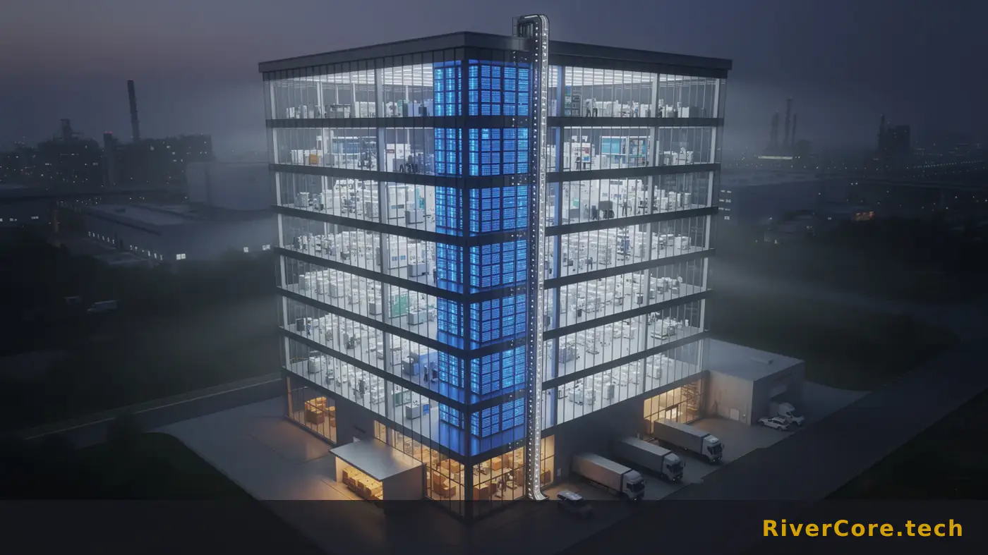
Samsung Bets 8,870 sqm at Onyang to Unclog HBM Backend
Anyone who has run a capacity-constrained backend knows what saturation looks like before the dashboards admit it: queue depth creeps, retries pile up, and every new feature fights the last one for headroom. Samsung's Cheonan advanced packaging center has hit that wall in physical form. The answer, according to Technetbook, is an eight-floor, 8,870 square meter fabrication build at the Onyang campus in Chungnam, converting a former test site into a full backend operational center.
The Numbers
Start with the footprint. 8,870 square meters across eight floors is not a line extension. It's a ground-up backend facility with a total area more than four times the size of an international football pitch. In semiconductor terms, that's the kind of envelope you commit to when you expect a decade of throughput growth, not a two-year bridge.
Context matters here. Onyang was previously a testing facility. Samsung is converting it into a complete backend operational center that runs a wafer probe line alongside a packaging system in the same building. The current advanced packaging center at Cheonan has reached its space limits, and industry consensus reflected in the reporting says Cheonan is at saturation. Retrofitting legacy lines there is described as an inefficient and costly burden.
Read that last sentence like an SRE would. "Inefficient and costly burden" is the polite version of "we've tried to patch the old cluster and it's cheaper to stand up a new one." Production incidents I've seen in high-throughput platforms follow the exact same curve: once a facility, physical or logical, crosses its design envelope, incremental fixes get expensive faster than they get effective. Cheonan, by this account, is past that knee in the curve.
The other number worth holding onto is implicit. HBM packaging is the bottleneck determining AI semiconductor delivery schedules across the industry. When Samsung commits four football pitches of floor area to backend, it's telling you where the constraint actually lives. Front-end wafer capacity is not the pinch point right now. Stacking, thermal handling, and test-to-pack integration are. My take: the square footage is the least interesting thing in this announcement. The layout is the story.
What's Actually New
The genuinely new piece is the "single Space" approach. Samsung is co-locating wafer probe testing and final product packaging in one facility, with a feedback loop where test results directly determine packaging adjustments. That is a structural change to how backend runs, not a capacity story.
In conventional backend flows, probe and package live in separate buildings, often separate campuses, with logistics and batch handoffs between them. That's fine for commodity DRAM. It falls apart for HBM, where yields are brutally sensitive to thermal performance and structural precision during stacking. Every extra hop between test data and packaging decisions is latency, and latency in a feedback loop kills yield.
Teams I've worked with on latency-sensitive systems treat this as axiomatic: the closer your telemetry sits to the thing it controls, the faster you converge on a stable operating point. Samsung is applying the same logic to atoms. Probe data from the wafer line flows directly into packaging parameter changes in the same building. That shortens the learning cycle on a new HBM stack from weeks to, plausibly, days.
The second new element is architectural intent. The facility is designed to avoid existing machinery updates that would cause delays. Translation: Samsung isn't trying to make Onyang compatible with Cheonan's tooling generation. It's a clean-sheet backend, which means the equipment mix can target current HBM stack geometries without carrying forward compromises. That's a significant tell about how quickly HBM architectures are moving.
Third, and easy to miss: Onyang is positioned as the central hub for decentralized backend operations. Samsung is not consolidating. It's building a hub-and-spoke backend topology with Onyang as the anchor node. That's a different operational posture than "one big packaging plant."
What's Priced In for Engineering Teams
For anyone building on top of AI infrastructure, some of this is old news. HBM supply has been the gating factor on GPU availability for two years running. Every platform lead buying inference capacity already assumes packaging, not silicon, is the real constraint. The scale of Samsung's response is not a surprise.
What isn't priced in is the integration pattern. The single Space model, if it works, compresses the development cycle for new HBM generations. For downstream consumers, that means shorter gaps between HBM3E, HBM4, and whatever follows. Capacity planners budgeting GPU fleets on 18 to 24 month memory generation cycles may need to tighten that window.
Also underpriced: the yield implication. The facility is explicitly designed to impact production yield rates through the tight test-to-pack loop. In HBM, a few points of yield is the difference between a product line that prints money and one that strangles the fab. Fintech and iGaming teams don't care about yield curves directly, but they care about GPU spot prices, and those track HBM yield more closely than most procurement models admit.
The uncomfortable read: if Onyang delivers on yield and cycle time, Samsung's competitive position in AI memory tightens meaningfully against SK hynix and Micron. If it slips, the market stays supply-constrained longer, and inference costs for everyone downstream stay elevated into 2027.
Contrarian View
The consensus take is that co-locating probe and packaging is obviously correct and Samsung is catching up to physics. The contrarian view: integrated single-site backend is a concentration risk dressed up as an optimization.
Decentralized backend exists for a reason. When probe and pack live in separate facilities, a fire, a flood, a tooling recall, or a contamination event takes out one node, not the whole pipeline. Merging them into one building, however large, couples failure modes. Eight floors of integrated wafer probe and packaging is eight floors that share HVAC, power, cleanroom protocols, and a single site disaster radius.
Samsung is mitigating by making Onyang the hub of a decentralized backend network, not the only node. Fine. But production incidents I've seen in tightly coupled systems teach the same lesson every time: the feedback loop that makes you fast in the steady state is the same loop that propagates faults when something goes wrong. If the single Space philosophy is applied too aggressively across future sites, Samsung trades yield gains for fragility it won't notice until it matters.
My take: the design is right for this HBM generation. Whether it's right for the next one depends on how disciplined they are about keeping Onyang a hub and not a single point of failure.
Key Takeaways
- Samsung's 8,870 square meter, eight-floor Onyang build is a backend architecture bet, not just a capacity add. The layout matters more than the footprint.
- The "single Space" model co-locates wafer probe and packaging to shorten the test-to-pack feedback loop, targeting yield and cycle time on HBM stacks.
- Cheonan saturation is the real signal. When retrofitting legacy lines becomes a costly burden, you stand up a clean site instead of patching.
- Downstream AI infrastructure buyers should tighten HBM generation assumptions in capacity plans. Faster backend cycles compress GPU refresh windows.
- Watch for concentration risk. Integrated single-site backend boosts yield in steady state and couples failure modes when something breaks.
Frequently Asked Questions
Q: Why is Samsung moving HBM packaging from Cheonan to Onyang?
The Cheonan advanced packaging center has reached its space limits, and industry reports describe it as saturated. Retrofitting legacy lines at Cheonan is considered an inefficient and costly burden, so Samsung is standing up a clean-sheet backend facility at Onyang to avoid machinery updates that would delay HBM production.
Q: What does the "single Space" approach actually mean in engineering terms?
It means wafer probe testing and final product packaging run inside the same facility on coordinated lines. Test results feed directly into packaging adjustments, creating a tight feedback loop that targets thermal performance, structural precision, and production yield rates on HBM stacks.
Q: How does this affect AI infrastructure costs downstream?
HBM packaging is the current bottleneck on AI accelerator supply. If Onyang improves yield and shortens HBM generation cycles as designed, GPU availability and pricing ease over time. If execution slips, the market stays supply-constrained and inference costs remain elevated for downstream platforms.